There are many difference between an ASIC and FPGA however, this article attempts to explain the fundamental difference between an Application Specific Integrated Circuit (ASIC) and a Field Programmable Gate Array (FPGA).
Some basic understanding of digital logic design or boolean logic is required.
Let us take an example of the AND gate from the previous article.
VHDL:
out <= A AND B;
Verilog and SystemVerilog:
assign out = A & B;
Synthesis, in simple words, is a process where the HDL code is translated into a gate level netlist by an Electronic Design Automation (EDA) software tool. Here, the synthesis tool takes the HDL code and synthesis library containing logic cells/primitives/gates as input and creates a gate level logic circuit by mapping the HDL logic onto the available primtives.
ASIC
If we synthesise (not compile) the above VHDL, Verilog and SystemVerilog code, it would realise into the following logic gate inside an ASIC (assuming the ASIC synthesis library contains an AND gate cell:
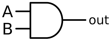
[Image source: https://lalacomputersci.wordpress.com/and-gate/]
However, if the ASIC library does not contain an AND gate but contains a NAND gate, the HDL code would realise into an AND gate using NAND gates:
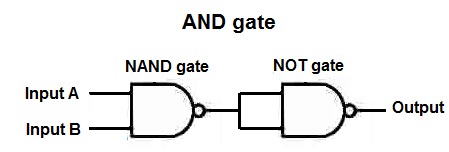
[Image source: http://www.learningaboutelectronics.com/Articles/AND-gate-from-NAND-gates-circuit.php]
This gate is further realised using CMOS transistors which are then etched on to a Silicon chip as shown in the previous article on this blog.
FPGA
How else can we create an AND gate if we do not have an actual AND gate CD4081 or an ASIC like the above? In order to answer the question, let us remind the truth table of an AND gate:
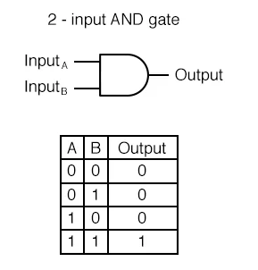
[Image Source: https://www.allaboutcircuits.com/textbook/digital/chpt-3/multiple-input-gates/]
If we can generate the output for a given input A and B as shown in the table above, we can have a functional AND gate.
Can you think of a logic block that can achieve this? Right, its a memory. So, if we store the above truth table in a RAM/ROM, we can have a functional AND gate without having an actual AND gate.
For example, let us take a memory with 1 bit wide data storage and 2 bit wide address. Then, let us store data 0 at the first address location 2’b00; 0 at the second location 2’b01; 0 at the third location 2’b10 and 1 at the fourth location 2’b11. Now let us connect the inputs A and B to the address bus of the RAM/ROM. So whenever the inputs A and B are both 1’s, the data stored at location 2’b11 will be provided at its output i.e. 1 otherwise the output will be data stored at other locations i.e. 0.
FPGAs implement combinatorial logic is using memories which are also called Look Up Tables (LUT). Any logic circuit for which a truth table is available, can be implemented using memory. It is this fundamental reason, FPGAs are reconfigurable which means, the same FPGA chip can realise different logic circuits without requiring to replace the actual chip. Modern FPGAs offer many other reconfigurable logic elements for example, routing between its elemental logic blocks etc. However, these other configurable aspects are out of scope of this article.
Memories such as LUTs, RAM, ROM are implemented on Silicon using transistors just like the above, it is hardware not software. Therefore, regardless of how an AND gate is implemented in an ASIC or FPGA, HDL code used to realise such a digital logic circuit is hardware not software!
FPGA synthesis tools implement the above RTL in a LUT. Therefore, whether you implement a 2 input OR gate or a 2 input AND gate, the schematic containing a LUT will appear the same after synthesis. It is what truth table the LUT is configured that makes the difference in its functional behaviour.
EMPIRICAL VALIDATION THROUGH LOGIC SIMULATION
Let us test the above hypothesis by implementing the logic in a digital logic Simulator like MultiMedia Logic which can be downloaded from https://sourceforge.net/projects/multimedialogic/
On the left side, the AND gate is created using two NAND gates and on the right hand side AND gate is created using a memory. The memory is stored with the values from the AND gate truth table and functions as a ROM. I have grounded the unused address lines since the simulator can only provide a memory model that has 8 bit address lines.
Here are the screenshots of the simulation that was created in the simulator. We are injecting 01 at the two inputs. You can observe that the LED is not lit.
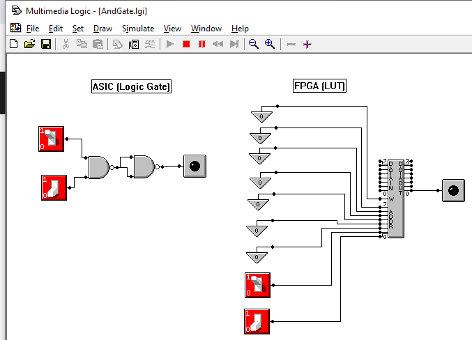
Now if we apply 1 to both inputs, the LED is lit like so:
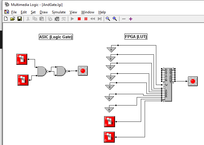
This proves that logically and functionally both circuits are same.
EMPIRICAL VALIDATION THROUGH CIRCUIT IMPLEMENTATION
I leave it to you to obtain an AND gate IC like CD4081, wire it on a breadboard and test it. Similarly, you can obtain a EEPROM in which you can store the truth-table of an AND gate as explained above and test the theory further.