While working on a European Research project called FASTMATCH where the project demonstration was carried out by implementing and intelligent high-speed Intrusion Detection System (IDS).
The demonstrator platform was a custom developed 14 layer electronic circuit board comprising of two Xilinx Virtex-5 FPGAs performing real-time line-rate string matching at 10Gbps.
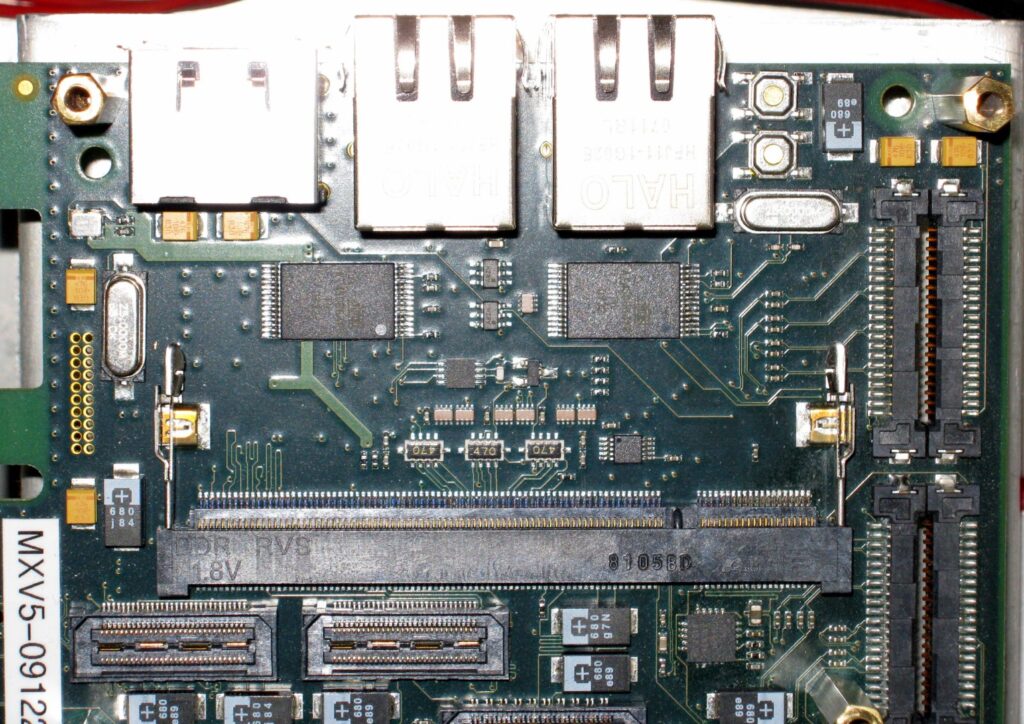
During our development, we noticed that we were not able to use the onboard DDR2 as the Xilinx projects kept on failing to access. Since failure was not an option, we started with tracing in the board schematics and deploying tools like JATGLive however we were unsuccessful.
Then, we created an RTL design in the FPGA which interfaced with the DDR2 and wrote known data to the memory, read it back and displayed it over a UART. While performing these writes and reads, one position of the data was not correct. This gave a hint that something was not right with the pins associated with the data. We then traced each pin of the DDR2-SODIMM socket to FPGA. We noticed that one of the DQ and DQS pins were swapped.
Then the question was, how to fix the board without damaging it. We then thought if some sort of DDR2 socket daughter board was available which can be modified by swapping those two pins instead of re-working the actual board. We tried looking for such a board and found a company who had developed a DDR2 daughter board or a riser board that would slot into the DDR2-SODIMM and would accept DDR2 memory. We found such a product called SODIMM Bend Back Riser from a company called ADEX electronics.
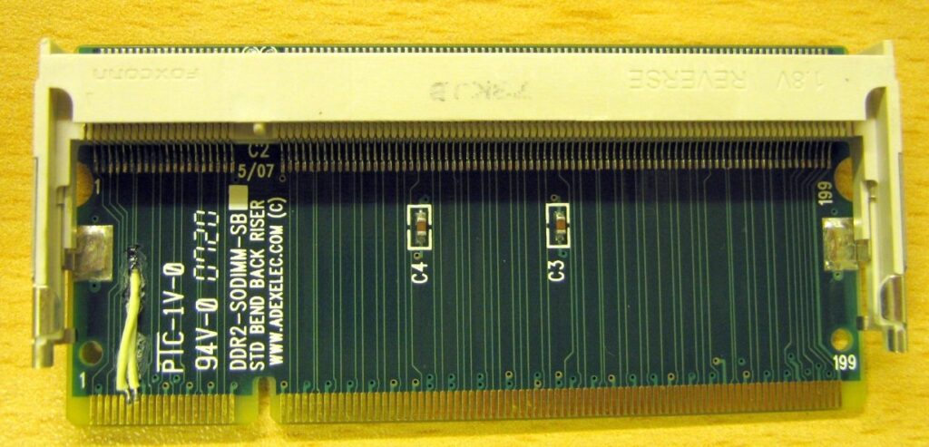
As you can see in the above picture, We then swapped those DQ and DQS pins back by cutting the tracks and soldering two wires. The DDR2 memory was fitted onto this riser board and the whole assembly was fit onto the FPGA board and wallah! The DDR2 came to life, We were even able to boot PetaLinux on Microblaze implemented on one of those Virtex-5 FPGAs :).